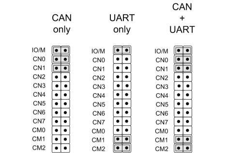
Figure 1: J4 Base Address Jumper with Option Default CAN Settings
The JANUS-MM board has the following jumper-selectable configuration options.
NOTE: In the figures in this section, jumpered pins are shown as a shaded connector.
This section presents the following configurable CAN options.
Use pin sets CN0-CN7 of jumper J4 to set the CAN base address using one of the following address spaces.
Note: The pin layout shows the default factory jumper settings for the CAN memory configuration options.
Figure 1: J4 Base Address Jumper with Option Default CAN Settings
| J4 | |
| Jumpered Pins | Function |
| IO/M | Out: Select I/O base address In: Select memory base address (default) |
If you have selected to access CAN through memory base addresses, the CAN memory base address is specified using eight jumpers, CN0-CN7, corresponding to address bits A10-A17, respectively.
| Jumper | CN7 | CN6 | CN5 | CN4 | CN3 | CN2 | CN1 | CN0 |
| Address bit | A17 | A16 | A15 | A14 | A13 | A12 | A11 | A10 |
Address bits A18 and A19 are always set; see the address mapping table, below, for the resulting base address values.
The following table shows the jumper-to-address mapping for memory space.
| Base Address | CN7 | CN6 | CN5 | CN4 | CN3 | CN2 | CN1 | CN0 |
| C0000h | In | In | In | In | In | In | In | In |
| C0400h | In | In | In | In | In | In | In | Out |
| C0800h | In | In | In | In | In | In | Out | In |
| C0C00h | In | In | In | In | In | In | Out | Out |
| C1000h | In | In | In | In | In | Out | In | In |
| C2000h | In | In | In | In | Out | In | In | In |
| C3000h | In | In | In | In | Out | Out | In | In |
| C4000h | In | In | In | Out | In | In | In | In |
| C5000h | In | In | In | Out | In | Out | In | In |
| C6000h | In | In | In | Out | Out | In | In | In |
| C7000h | In | In | In | Out | Out | Out | In | In |
| C8000h | In | In | Out | In | In | In | In | In |
| C9000h | In | In | Out | In | In | Out | In | In |
| CA000h | In | In | Out | In | Out | In | In | In |
| CB000h | In | In | Out | In | Out | Out | In | In |
| CC000h | In | In | Out | Out | In | In | In | In |
| CD000h | In | In | Out | Out | In | Out | In | In |
| CE000h | In | In | Out | Out | Out | In | In | In |
| CF000h | In | In | Out | Out | Out | Out | In | In |
| D0000h | In | Out | In | In | In | In | In | In |
| D1000h | In | Out | In | In | In | Out | In | In |
| D2000h | In | Out | In | In | Out | In | In | In |
| D3000h | In | Out | In | In | Out | Out | In | In |
| D4000h | In | Out | In | Out | In | In | In | In |
| D5000h | In | Out | In | Out | In | Out | In | In |
| D6000h | In | Out | In | Out | Out | In | In | In |
| D7000h | In | Out | In | Out | Out | Out | In | In |
| D8000h | In | Out | Out | In | In | In | In | In |
| D8400h | In | Out | Out | In | In | In | In | Out |
| D8800h | In | Out | Out | In | In | In | Out | In |
| D8C00h | In | Out | Out | In | In | In | Out | Out |
| D9000h | In | Out | Out | In | In | Out | In | In |
| DA000h | In | Out | Out | In | Out | In | In | In |
| DB000h | In | Out | Out | In | Out | Out | In | In |
| DC000h | In | Out | Out | Out | In | In | In | In |
| DD000h | In | Out | Out | Out | In | Out | In | In |
| DE000h | In | Out | Out | Out | Out | In | In | In |
| DF000h | In | Out | Out | Out | Out | Out | In | In |
| E0000h | Out | In | In | In | In | In | In | In |
| E1000h | Out | In | In | In | In | Out | In | In |
| E2000h | Out | In | In | In | Out | In | In | In |
| E3000h | Out | In | In | In | Out | Out | In | In |
| E4000h | Out | In | In | Out | In | In | In | In |
| E5000h | Out | In | In | Out | In | Out | In | In |
| E6000h | Out | In | In | Out | Out | In | In | In |
| E7000h | Out | In | In | Out | Out | Out | In | In |
| E8000h | Out | In | Out | In | In | In | In | In |
| E9000h | Out | In | Out | In | In | Out | In | In |
| EA000h | Out | In | Out | In | Out | In | In | In |
| EB000h | Out | In | Out | In | Out | Out | In | In |
| EC000h | Out | In | Out | Out | In | In | In | In |
| ED000h | Out | In | Out | Out | In | Out | In | In |
| EE000h | Out | In | Out | Out | Out | In | In | In |
| EF000h | Out | In | Out | Out | Out | Out | In | In |
| F0000h | Out | Out | In | In | In | In | In | In |
| F1000h | Out | Out | In | In | In | Out | In | In |
| F2000h | Out | Out | In | In | Out | In | In | In |
| F3000h | Out | Out | In | In | Out | Out | In | In |
| F4000h | Out | Out | In | Out | In | In | In | In |
| F5000h | Out | Out | In | Out | In | Out | In | In |
| F6000h | Out | Out | In | Out | Out | In | In | In |
| F7000h | Out | Out | In | Out | Out | Out | In | In |
| F8000h | Out | Out | Out | In | In | In | In | In |
| F9000h | Out | Out | Out | In | In | Out | In | In |
| FA000h | Out | Out | Out | In | Out | In | In | In |
| FB000h | Out | Out | Out | In | Out | Out | In | In |
| FC000h | Out | Out | Out | Out | In | In | In | In |
| FD000h | Out | Out | Out | Out | In | Out | In | In |
| FE000h | Out | Out | Out | Out | Out | In | In | In |
| FF000h default | Out | Out | Out | Out | Out | Out | In | In |
| FF400h | Out | Out | Out | Out | Out | Out | In | Out |
| FF800h | Out | Out | Out | Out | Out | Out | Out | In |
| FFC00h | Out | Out | Out | Out | Out | Out | Out | Out |
Note: Address bits A18 and A19 have a value of one (1).
The base address is specified for CAN port A. The base address for CAN port B is located at port A base address + 00200h, as shown in the following table.
| CAN Port | Base Address |
| A | (Jumpered base address) |
| B | (Jumpered base address) + 00200h |
For example, to configure the memory base address of port A to D0000h, jumper IO/M, CN0-CN5 and CN7. The base address of port B is then D0200h. The example is shown in the following figure.
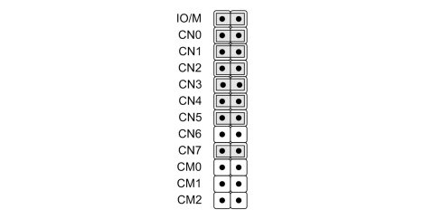
Figure 2: Memory Base Address Selection Example
Reset ports A and B by writing to any of the memory addresses shown in the following table.
| CAN Port | CAN Reset Address Range |
| A | 00100h – 001FFh |
| B | 00300h – 003FFh |
If you have selected I/O addressing to access the CAN controllers, the CAN controller have a 64-byte I/O address space (32 bytes per port). The I/O base address is specified using four jumpers,CN0-CN3, corresponding to I/O address bits A9-A6, respectively.
| Jumper | CN3 | CN2 | CN1 | CN0 |
| Address bit | A9 | A8 | A7 | A6 |
| Base Address | CN3 | CN2 | CN1 | CN0 |
| 0000h | In | In | In | In |
| 0040h | In | In | In | Out |
| 0080h | In | In | Out | In |
| 00C0h | In | In | Out | Out |
| 0100h | In | Out | In | In |
| 0140h | In | Out | In | Out |
| 0180h | In | Out | Out | In |
| 01C0h | In | Out | Out | Out |
| 0200h | Out | In | In | In |
| 0240h | Out | In | In | Out |
| 0280h | Out | In | Out | In |
| 02C0h | Out | In | Out | Out |
| 0300h | Out | Out | In | In |
| 0340h | Out | Out | In | Out |
| 0380h | Out | Out | Out | In |
| 03C0h | Out | Out | Out | Out |
Note: Address bits A11-A15 have a value of zero (0).
The I/O base address is specified for CAN port A. The I/O base address for CAN port B is located at port A I/O base address + 0020h, as shown in the following table.
| CAN Port | Base Address |
| A | (Jumpered I/O base address) |
| B | (Jumpered I/O base address) + 0020h |
Use jumper J5 to specify the IRQ for both CAN ports. The following diagram shows the jumper pin layout.
(The default jumper settings shown in the diagram apply to the CAN+UART and CAN-only configuration options).
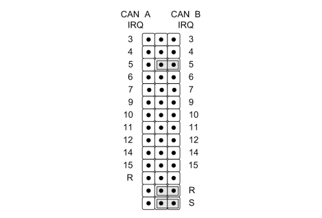
Figure 3: J5 Jumper with Default Settings
The pin label corresponds to the IRQ (IRQ3-IRQ7, IRQ9-IRQ12, IRQ14, IRQ15).
The center column of pins corresponds to the IRQ. Assign the IRQ to CAN port A (CAN A) by shorting the center pin and the pin to its left. Similarly, assign the IRQ to CAN port B (CAN B) by shorting the center pin and the pin to its right. In the diagram, above, IRQ4 is assigned to CAN port A and IRQ3 is assigned to CAN port B.
To share the same IRQ on both CAN ports A and B, short the pin labeled ‘S’ to its corresponding center pin, and jumper the desired IRQ for either CAN ports A or B. Refer to for an example of the use of the ‘S’ pin.
To associate the pull-down resistor on this board with the IRQ for the CAN port, short the ‘R’ pin of the CAN port and the center pin.
Note: Only one pull-down resistor is allowed per IRQ in the entire PC/104 stack.
Jumpers J10 and J11 provide CAN termination, slew rate and power supply selection for both CAN ports; J10 is used to configure CAN port A and J11 is used to configure CAN port B. The following diagram shows the jumper pin layout.
(The default jumper settings shown in the diagram apply to the CAN+UART and CAN-only configuration options).

Figure 4: J10 and J11 Jumpers with Default Settings
| Jumpered Pins | Function |
| T | CAN termination. In: Board terminates CAN bus (default). Out: Board does not terminate CAN bus. |
| SR | Slew rate selection. In: High-speed operating mode. Out: Slope-controlled operating mode (default). |
CG CP LP |
CAN power supply selection. GND from CAN +5V from CAN; power supply over CAN bus powers the local port (default) +5V from DCP; local isolated power supply is used to power the CAN bus (default) |
Shorting the CAN termination jumper (T) puts a 120-Ohm resistor between CANL and CANH.
Note: The CAN bus should be terminated only at the ends of the bus, for a maximum of two terminations on the bus.
CAN Slew RateFor high-speed operation, the transmitter output transistors are switched on and off as fast as possible. In this mode, the rise and fall slope is not limited. Use of a shielded cable is recommended to avoid RFI problems. The slope control operating mode allows the use of an unshielded twisted pair or a parallel pair of wires as bus lines by programming the rise and fall slope with a resistor connected to ground.
Short the slew rate jumper (SR) to select high-speed operating mode.
CAN Power Supply SelectionBecause the CAN ports and transceivers are isolated, it is possible that two different ports will not communicate properly if the voltage differential is too great. The J10/J11 jumpers (CG, CP, LP) are provided to attach/remove these power rails. One way to ensure that the two ends of the CAN communication are within voltage range is to share the same ground, or use one power supply for both terminals. Also, the local supply may be used to power the bus, and the local port may be powered from the bus.
The following options are provided to attach/remove the power rails.
The following figure shows the jumper settings for the power supply options.
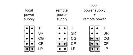
Figure 5: Power Supply Selection Example
The UART is a dual port device that connects to GPS serial port 1 and to either GPS serial port 2 or the SocketModemTM, depending on the application.
This section presents the following UART configuration topics.
The base address uniquely assigns the UART address within the PC/104 system. Use pin sets CM0, CM1 and CM2 of jumper J4 to set the UART base address.
Note: The pin layout shows the default factory jumper settings for the dual UART memory configuration options. (The IO/M jumper only applies to CAN memory addressing).
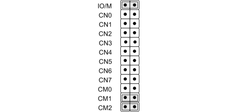 Figure 6: J4 Base Address Jumper with Option Default UART Settings
| UART port A Base Address |
UART port B Base Address |
CM2 | CM1 | CM0 |
| 03F8h | 02F8h | In | In | In |
| 03E8h | 02E8h | In | In | Out |
| 0380h | 0388h | In | Out | In |
| 0240h | 0248h | In | Out | Out |
| 0100h | 0108h | Out | In | In |
| 0120h | 0128h | Out | In | Out |
| 0140h | 0148h | Out | Out | In |
| 0160h | 0168h | Out | Out | Out |
The UART can be configured to generate interrupts using a particular IRQ with the PC/104 system.
Use jumper J6 to select the IRQ for both UARTs. The following diagram shows the jumper pin layout.
Note: The default jumper settings shown in the diagram apply to the CAN+UART and UART-only configuration options.
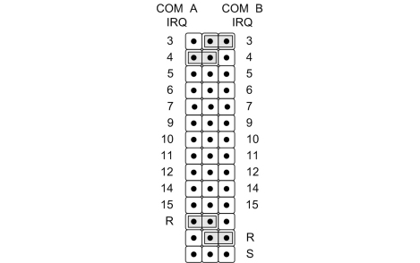 Figure 7: J6 Jumper with Default Settings
The pin label corresponds to the selectable IRQ (IRQ3-IRQ7, IRQ9-IRQ12, IRQ14, IRQ15).
The center column of pins corresponds to the IRQ. Assign the IRQ to UART A (COM A) by shorting the center pin and the pin to its left. Similarly, assign the IRQ to UART port B (COM B) by shorting the center pin and the pin to its right. In the diagram, above, IRQ4 is assigned to UART A and IRQ3 is assigned to UART port B.
 Figure 8: Shared IRQ Selection
To share the same IRQ on both UARTs A and B, short the pin labeled ‘S’ to its corresponding center pin, and jumper the desired IRQ for either UARTs A or B. In the example, below, IRQ 14 is assigned to both UART A and UART B.
Note: Only one pull-down resistor is allowed per IRQ in the entire PC/104 stack.
UART serial port B can be used to communicate with either a GPS receiver, for applications that require two GPS receivers, or the SocketModemTM.
Jumper J9 provides the mechanism for selecting UART port B to communicate with either the SocketModemTM or GPS, and for selection the modem power option.
The following power options are provided.
Note: The default jumper settings shown in the diagram apply to the CAN+UART and UART-only options.
 Figure 9: J9 Jumper with Default Settings
| Jumpered Pins | Function |
| MDM (pair) | Bottom position: Socket modem transmit (Tx) (default) Top position: Socket modem receive (Rx) (default) |
| GPS (pair) | Bottom position: GPS port 2 transmit (Tx) Top position: GPS port 2 receive (Rx) |
| 3V3 | Select +3.3V modem power |
| 5V | Select +5V modem power (default) |
Note: The transmit (Tx) and receive (Rx) pair of jumpers must both select either MDM or GPS.
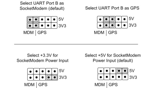 Figure 10: Socket Modem/GPS and Modem Power Selection
Either the Trimble Lassen SKIITM or iQTM GPS modules may be installed. The different GPS modules require different voltages, which are configurable using jumper J16.
The following figure shows the jumper configuration for the GPS power options.
 Figure 11: GPS Power Option Configuration